Can someone help me to connect this PCM5102 to Vim1? A pins little different from topicstarter’s one… 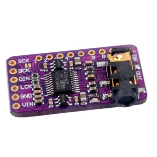
SCK --> PIN29 / I2S_SCK
DIN --> PIN31 / I2S_SDO
LCK --> PIN32 / I2S_LCK
GND --> PIN28 / GND
VIN --> PIN27 / VCC3.3V
Enjoy!
3 Likes
Thanks Gouwa! At first it didn’t worked but I’ve also connected BCK to pin 30.
SCK → PIN29 / I2S_SCK
BCK → PIN30
DIN → PIN31 / I2S_SDO
LCK → PIN32 / I2S_LCK
GND → PIN28 / GND
VIN → PIN27 / VCC3.3V
2 Likes
I think need to connect SCK to 30pin and BCK to 29pin .
can someone help me. I have a vim 2g/8g with libreelec 8.2.3.1 in mmc, but there is no chance to get the i2s signal. The connection is BCK <> GPIOH_7 (pin 29), DATA <> GPIOAO_9 (pin 31),LRCK <> GPIOH_8 (pin 32), gnd is pin 28. With the vim2 it works, but here no chance.
What can i do ? Thanks
So if we have a i2C dac we can hook it up on the vim2 and it will work?
YES! this one proper connection for i2s DAC
| SIGNAL | PIN | PIN | SIGNAL | DAC |
|---|---|---|---|---|
| 5V | 1 | 21 | GND | |
| 5V | 2 | 22 | I2C_M3_SCL | |
| USB_DM | 3 | 23 | I2C_M3_SDA | |
| USB_DP | 4 | 24 | GND | |
| GND | 5 | 25 | I2C_AO_SCK | |
| VCC_MCU | 6 | 26 | I2C_AO_SDA | |
| MCU_NRST | 7 | 27 | 3.3V | |
| MCU_SWIM | 8 | 28 | GND → | GND |
| GND | 9 | 29 | I2SB_SCLK → | BCK |
| ADC_CH0 | 10 | 30 | I2S_MCLK0 | |
| 1.8V | 11 | 31 | I2SB_SDO → | DATA |
| ADC_CH3 | 12 | 32 | I2SB_LRCK → | LRCK |
| SPDIF_OUT | 13 | 33 | I2SB_SDI | |
| GND | 14 | 34 | GND | |
| UARTC_RX | 15 | 35 | PWM_F | |
| UARTC_TX | 16 | 36 | RTC_CLK | |
| GND | 17 | 37 | GPIOH_4 | |
| Linux_RX | 18 | 38 | MCU_PA1 | |
| Linux_TX | 19 | 39 | GPIODZ_15 | |
| 3.3V | 20 | 40 | GND |
2 Likes
To make this DAC work in ubuntu/linux, did you have to modify any config file or it just works by just connecting the board and it appears in sound output options?
@Yasir_Javed after connecting the DAC, you might need to specify the audio sink to I2S, but I think it should work automatically
1 Like
Hello,
Just to point out that in my case I had to invert bck and sck (compared to @Gouwa message) to make it work in my pcm5102
so I connected
SCK → PIN30
BCK → PIN29
DIN → PIN31 / I2S_SDO
LCK → PIN32 / I2S_LCK
GND → PIN28 / GND
VIN → PIN27 / VCC3.3V
Putting SCK on a ground pin also works (it will use internal clock)