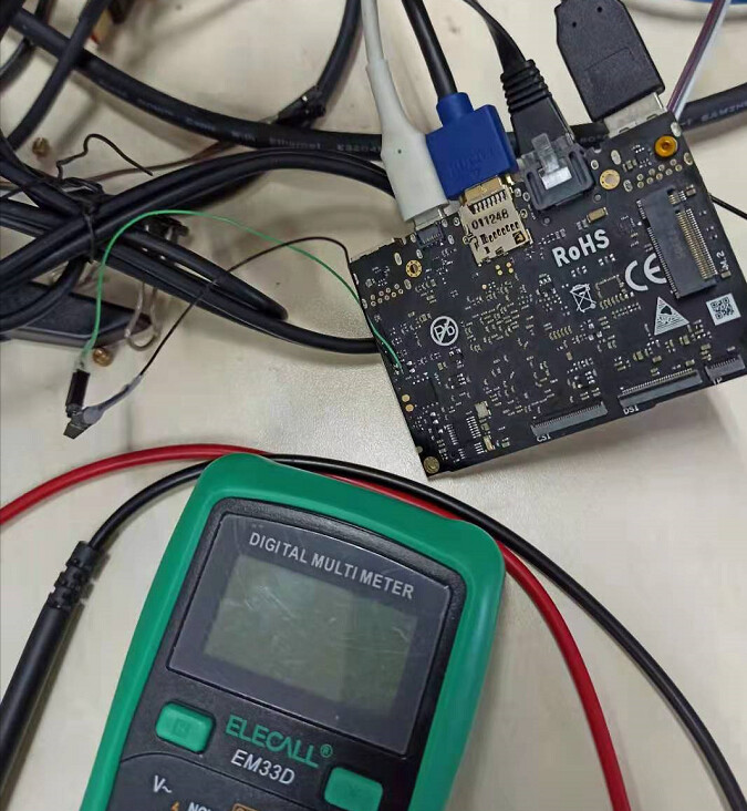
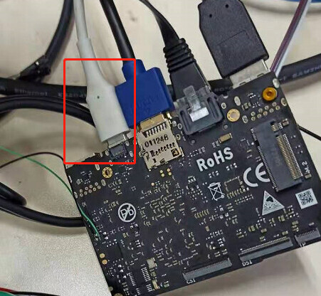
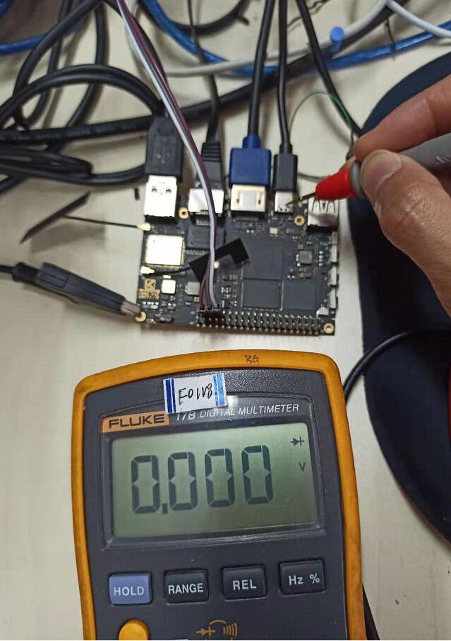
@Frank The white cable is the normal Type C with data transmission as I use it to transfer data with my Phone.
Also, I tried another TypeC data wire, it also not working. Furthermore, I tried 2 computers(one is the Windows, another is the Ubuntu).
A question:
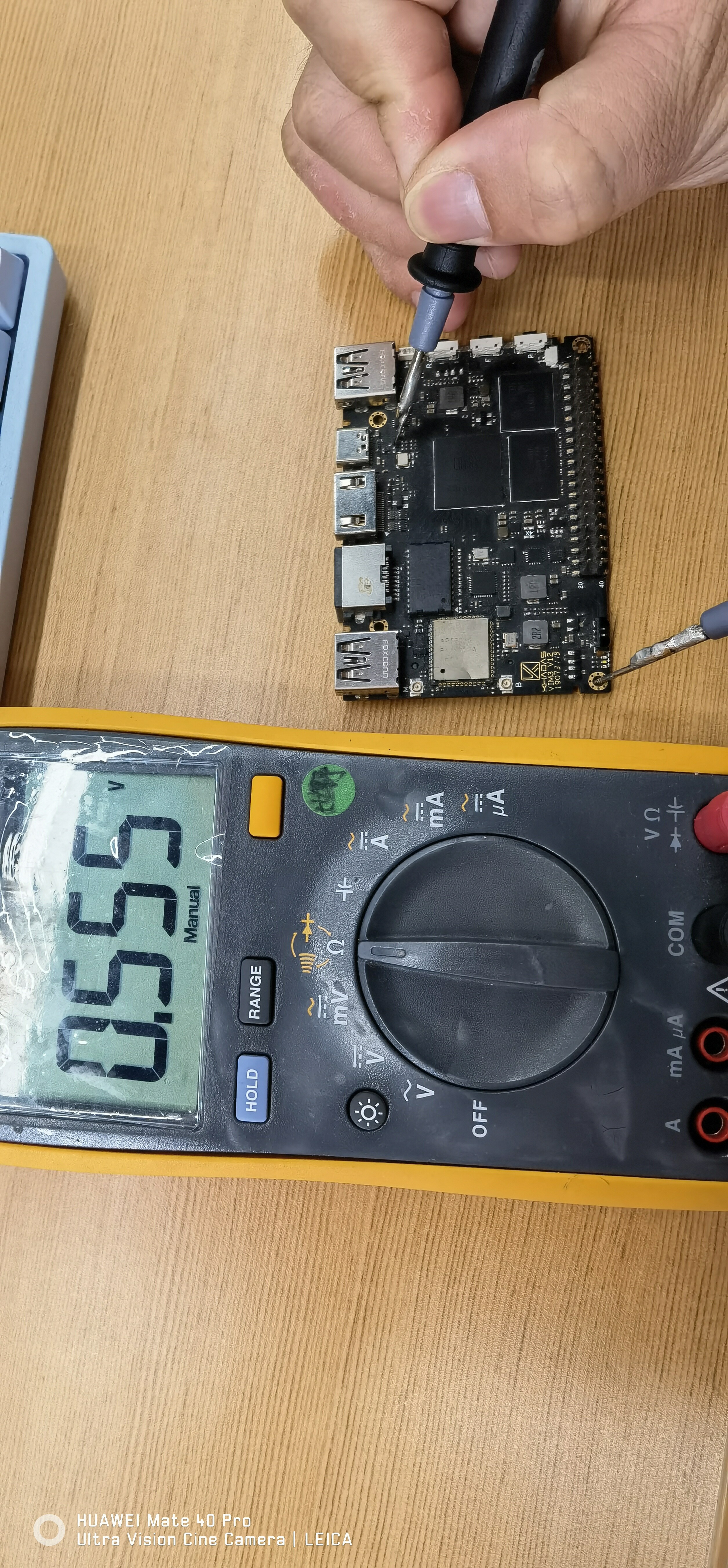
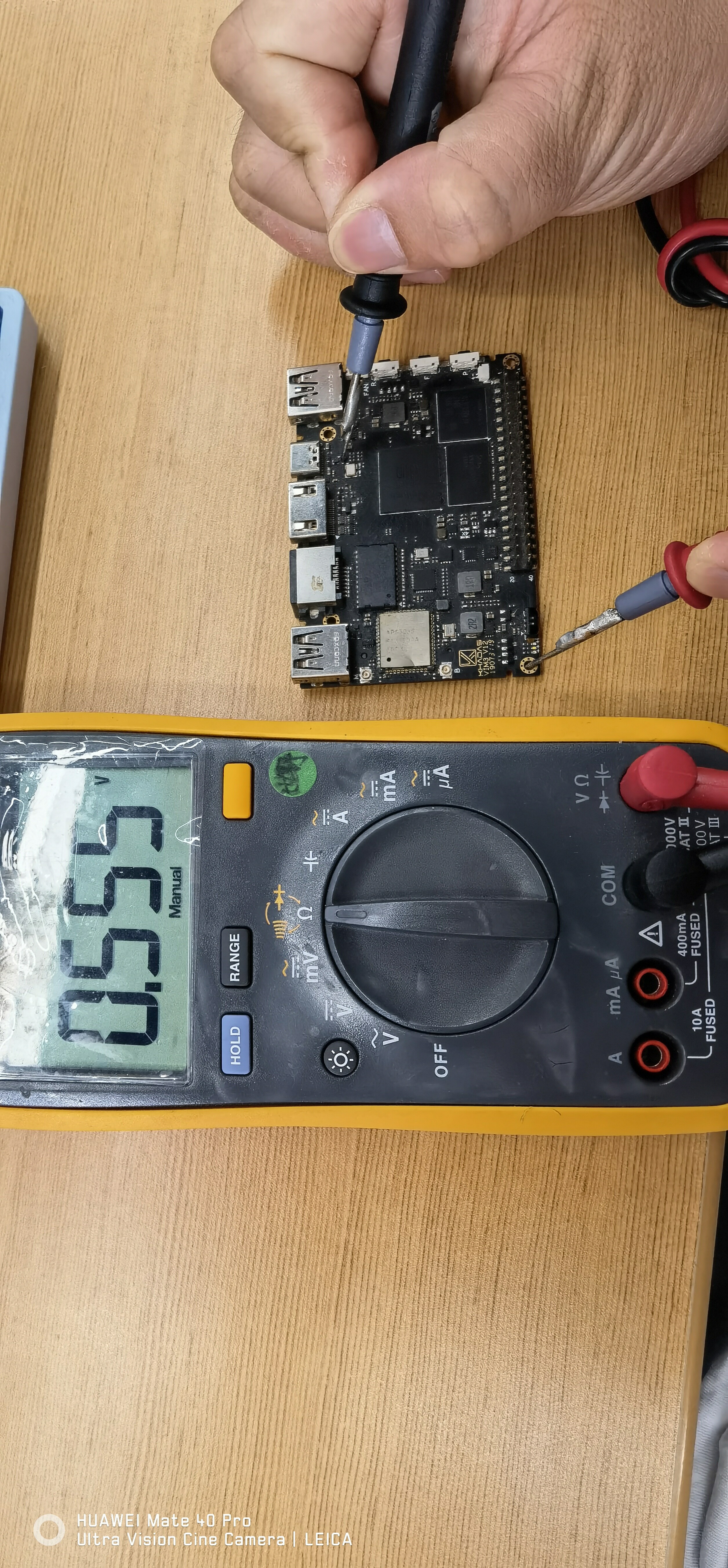
Why the board cann’t enter the upgrade mode when MRegister pads are connected ?
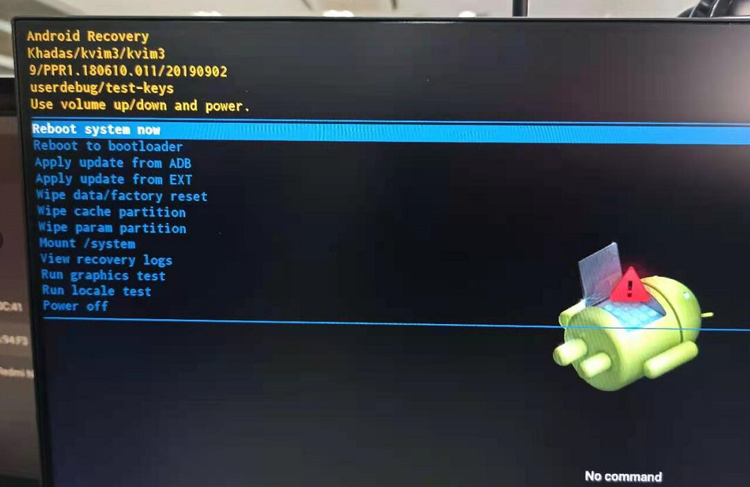
Following is the bootlog with TST mode key preseed:
G12B:BL:6e7c85:2a3b91;FEAT:E0F83180:402000;POC:D;RCY:0;USB:0;EMMC:0;READ:0;0.
bl2_stage_init 0x01
bl2_stage_init 0x81
hw id: 0x0000 - pwm id 0x01
bl2_stage_init 0xc1
bl2_stage_init 0x02

L0:00000000
L1:20000703
L2:00008067
L3:14000000
B2:00402000
B1:e0f83180

TE: 307733

BL2 Built : 19:22:01, Jul 31 2019. g12b ge9a9000 - zhiguang.ouyang@droid07-sz

Board ID = 8
Set A53 clk to 24M
Set A73 clk to 24M
Set clk81 to 24M
A53 clk: 1200 MHz
A73 clk: 1200 MHz
CLK81: 166.6M
smccc: 0004fc00
eMMC boot @ 0
sw8 s
DDR driver_vesion: LPDDR4_PHY_V_0_1_18 build time: Jul 31 2019 19:21:56
board id: 8
Load FIP HDR from eMMC, src: 0x00010200, des: 0xfffd0000, size: 0x00004000, part: 0
fw parse done
Load ddrfw from eMMC, src: 0x00060200, des: 0xfffd0000, size: 0x0000c000, part: 0
Load ddrfw from eMMC, src: 0x00038200, des: 0xfffd0000, size: 0x00004000, part: 0
PIEI prepare done
fastboot data load
00000000
emmc switch 1 ok
ddr saved addr:00016000
Load ddr parameter from eMMC, src: 0x02c00000, des: 0xfffd0000, size: 0x00001000, part: 0
00000000
emmc switch 0 ok
fastboot data verify
verify result: 265
Cfg max: 4, cur: 1. Board id: 255. Force loop cfg
LPDDR4 probe
ddr clk to 1608MHz
Load ddrfw from eMMC, src: 0x0003c200, des: 0xfffd0000, size: 0x0000c000, part: 0

dmc_version 0001
Check phy result
INFO : ERROR : Training has failed!
1D training failed
Cfg max: 4, cur: 2. Board id: 255. Force loop cfg
LPDDR4 probe
ddr clk to 1608MHz
Load ddrfw from eMMC, src: 0x0003c200, des: 0xfffd0000, size: 0x0000c000, part: 0

dmc_version 0001
Check phy result
INFO : End of CA training
INFO : End of initialization
INFO : Training has run successfully!
Check phy result
INFO : End of initialization
INFO : End of read enable training
INFO : End of fine write leveling
INFO : End of Write leveling coarse delay
INFO : Training has run successfully!
Check phy result
INFO : End of initialization
INFO : End of read dq deskew training
INFO : End of MPR read delay center optimization
INFO : End of write delay center optimization
INFO : End of read delay center optimization
INFO : End of max read latency training
INFO : Training has run successfully!
1D training succeed
Load ddrfw from eMMC, src: 0x00048200, des: 0xfffd0000, size: 0x0000c000, part: 0
Check phy result
INFO : End of initialization
INFO : End of 2D read delay Voltage center optimization
INFO : End of 2D read delay Voltage center optimization
INFO : End of 2D write delay Voltage center optimization
INFO : End of 2D write delay Voltage center optimization
INFO : Training has run successfully!

channel==0
RxClkDly_Margin_A0==77 ps 8
TxDqDly_Margin_A0==106 ps 11
RxClkDly_Margin_A1==0 ps 0
TxDqDly_Margin_A1==0 ps 0
TrainedVREFDQ_A0==29
TrainedVREFDQ_A1==0
VrefDac_Margin_A0==28
DeviceVref_Margin_A0==29
VrefDac_Margin_A1==0
DeviceVref_Margin_A1==0


channel==1
RxClkDly_Margin_A0==97 ps 10
TxDqDly_Margin_A0==106 ps 11
RxClkDly_Margin_A1==0 ps 0
TxDqDly_Margin_A1==0 ps 0
TrainedVREFDQ_A0==29
TrainedVREFDQ_A1==0
VrefDac_Margin_A0==29
DeviceVref_Margin_A0==28
VrefDac_Margin_A1==0
DeviceVref_Margin_A1==0

 dwc_ddrphy_apb_wr((0<<20)|(2<<16)|(0<<12)|(0xb0):0004

soc_vref_reg_value 0x 0G12B:BL:6e7c85:2a3b91;FEAT:E0F83180:402000;POC:D;RCY:0;USB:0;EMMC:0;READ:0;0.2_stage_init 0x01
bl2_stage_init 0x81
hw id: 0x0000 - pwm id 0x01
bl2_stage_init 0xc1
bl2_stage_init 0x02

L0:00000000
L1:20000703
L2:00008067
L3:14000000
B2:00402000
B1:e0f83180

TE: 180670

BL2 Built : 19:22:01, Jul 31 2019. g12b ge9a9000 - zhiguang.ouyang@droid07-sz

Board ID = 8
Set A53 clk to 24M
Set A73 clk to 24M
Set clk81 to 24M
A53 clk: 1200 MHz
A73 clk: 1200 MHz
CLK81: 166.6M
smccc: 00030ba9
eMMC boot @ 0
sw8 s
DDR driver_vesion: LPDDR4_PHY_V_0_1_18 build time: Jul 31 2019 19:21:56
board id: 8
Load FIP HDR from eMMC, src: 0x00010200, des: 0xfffd0000, size: 0x00004000, part: 0
fw parse done
Load ddrfw from eMMC, src: 0x00060200, des: 0xfffd0000, size: 0x0000c000, part: 0
Load ddrfw from eMMC, src: 0x00038200, des: 0xfffd0000, size: 0x00004000, part: 0
PIEI prepare done
fastboot data load
00000000
emmc switch 1 ok
ddr saved addr:00016000
Load ddr parameter from eMMC, src: 0x02c00000, des: 0xfffd0000, size: 0x00001000, part: 0
00000000
emmc switch 0 ok
fastboot data verify
verify result: 265
Cfg max: 4, cur: 1. Board id: 255. Force loop cfg
LPDDR4 probe
ddr clk to 1608MHz
Load ddrfw from eMMC, src: 0x0003c200, des: 0xfffd0000, size: 0x0000c000, part: 0

dmc_version 0001
Check phy result
INFO : ERROR : Training has failed!
1D training failed
Cfg max: 4, cur: 2. Board id: 255. Force loop cfg
LPDDR4 probe
ddr clk to 1608MHz
Load ddrfw from eMMC, src: 0x0003c200, des: 0xfffd0000, size: 0x0000c000, part: 0

dmc_version 0001
Check phy result
INFO : End of CA training
INFO : End of initialization
INFO : Training has run successfully!
Check phy result
INFO : End of initialization
INFO : End of read enable training
INFO : End of fine write leveling
INFO : End of Write leveling coarse delay
INFO : Training has run successfully!
Check phy result
INFO : End of initialization
INFO : End of read dq deskew training
INFO : End of MPR read delay center optimization
INFO : End of write delay center optimization
INFO : End of read delay center optimization
INFO : End of max read latency training
INFO : Training has run successfully!
1D training succeed
Load ddrfw from eMMC, src: 0x00048200, des: 0xfffd0000, size: 0x0000c000, part: 0
Check phy result
INFO : End of initialization
INFO : End of 2D read delay Voltage center optimization
INFO : End of 2D read delay Voltage center optimization
INFO : End of 2D write delay Voltage center optimization
INFO : End of 2D write delay Voltage center optimization
INFO : Training has run successfully!

channel==0
RxClkDly_Margin_A0==97 ps 10
TxDqDly_Margin_A0==106 ps 11
RxClkDly_Margin_A1==0 ps 0
TxDqDly_Margin_A1==0 ps 0
TrainedVREFDQ_A0==29
TrainedVREFDQ_A1==0
VrefDac_Margin_A0==28
DeviceVref_Margin_A0==29
VrefDac_Margin_A1==0
DeviceVref_Margin_A1==0


channel==1
RxClkDly_Margin_A0==106 ps 11
TxDqDly_Margin_A0==106 ps 11
RxClkDly_Margin_A1==0 ps 0
TxDqDly_Margin_A1==0 ps 0
TrainedVREFDQ_A0==28
TrainedVREFDQ_A1==0
VrefDac_Margin_A0==29
DeviceVref_Margin_A0==28
VrefDac_Margin_A1==0
DeviceVref_Margin_A1==0

 dwc_ddrphy_apb_wr((0<<20)|(2<<16)|(0<<12)|(0xb0):0004

soc_vref_reg_value 0x 00000026 00000026 00000025 00000026 00000027 00000028 00000026 00000026 00000024 00000025 00000026 00000028 00000026 00000026 00000026 00000024 00000024 00000022 00000025 00000025 00000024 00000023 00000023 00000023 00000025 00000026 00000024 00000024 00000026 00000024 00000024 00000025 dram_vref_reg_value 0x 00000013
2D training succeed
aml_ddr_fw_vesion: LPDDR4_PHY_V_0_1_18 build time: Jul 31 2019 19:22:05
auto size-- 65535DDR cs0 size: 2048MB
DDR cs1 size: 0MB
DMC_DDR_CTRL: 00c0002cDDR size: 2048MB
cs0 DataBus test pass
cs0 AddrBus test pass

100bdlr_step_size ps== 478
result report
boot times 0Enable ddr reg access
00000000
emmc switch 3 ok
Authentication key not yet programmed
get rpmb counter error 0x00000007
00000000
emmc switch 0 ok
Load FIP HDR from eMMC, src: 0x00010200, des: 0x01700000, size: 0x00004000, part: 0
Load BL3X from eMMC, src: 0x00078200, des: 0x01768000, size: 0x000d7a00, part: 0
0.0;M3 CHK:0;cm4_sp_mode 0
MVN_1=0x00000000
MVN_2=0x00000000
[Image: g12b_v1.1.3389-92241b5 2019-07-02 17:23:01 luan.yuan@droid15-sz]
OPS=0x10
ring efuse init
chipver efuse init
29 0b 10 00 01 17 1a 00 00 02 37 30 4e 42 4e 50
[0.018961 Inits done]
secure task start!
high task start!
low task start!
run into bl31
NOTICE:  BL31: v1.3(release):4fc40b1
NOTICE:  BL31: Built : 15:58:17, May 22 2019
NOTICE:  BL31: G12A normal boot!
NOTICE:  BL31: BL33 decompress pass
ERROR:   Error initializing runtime service opteed_fast


U-Boot 2015.01-g3f780c9 (Sep 02 2019 - 07:56:22)

DRAM:  2 GiB
Relocation Offset is: 76e2c000
spi_post_bind(spifc): req_seq = 0
register usb cfg[0][1] = 0000000077f2e640
aml_i2c_init_port init regs for 0
NAND:  get_sys_clk_rate_mtd() 290, clock setting 200!
NAND device id: 0 9f df df df df
No NAND device found!!!
nand init failed: -6
get_sys_clk_rate_mtd() 290, clock setting 200!
NAND device id: 0 9f df df df df
No NAND device found!!!
nand init failed: -6
MMC:   aml_priv->desc_buf = 0x0000000073e1ca70
aml_priv->desc_buf = 0x0000000073e1edb0
SDIO Port B: 0, SDIO Port C: 1
co-phase 0x3, tx-dly 0, clock 400000
co-phase 0x3, tx-dly 0, clock 400000
co-phase 0x3, tx-dly 0, clock 400000
emmc/sd response timeout, cmd8, status=0x3df2800
emmc/sd response timeout, cmd55, status=0x3df2800
co-phase 0x3, tx-dly 0, clock 400000
co-phase 0x1, tx-dly 0, clock 40000000
aml_sd_retry_refix[983]:delay = 0x0,gadjust =0x2000
[mmc_startup] mmc refix success
init_part() 297: PART_TYPE_AML
[mmc_init] mmc init success
start dts,buffer=0000000073e21620,dt_addr=0000000073e21620
get_partition_from_dts() 91: ret 0
parts: 17
00:      logo   0000000000800000 1
01:  recovery   0000000001800000 1
02:      misc   0000000000800000 1
03:      dtbo   0000000000800000 1
04:  cri_data   0000000000800000 2
05:     param   0000000001000000 2
06:      boot   0000000001000000 1
set has_boot_slot = 0
07:       rsv   0000000001000000 1
08:  metadata   0000000001000000 1
09:    vbmeta   0000000000200000 1
10:       tee   0000000002000000 1
11:    vendor   0000000014000000 1
12:       odm   0000000008000000 1
13:    system   0000000050000000 1
14:   product   0000000008000000 1
15:     cache   0000000046000000 2
16:      data   ffffffffffffffff 4
init_part() 297: PART_TYPE_AML
eMMC/TSD partition table have been checked OK!
crc32_s:0x1577dad == storage crc_pattern:0x1577dad!!!
crc32_s:0xee152b83 == storage crc_pattern:0xee152b83!!!
crc32_s:0x79f50f07 == storage crc_pattern:0x79f50f07!!!
mmc env offset: 0x4d400000
In:    serial
Out:   serial
Err:   serial
reboot_mode=cold_boot
[store]To run cmd[emmc dtb_read 0x1000000 0x40000]
_verify_dtb_checksum()-3406: calc 438c7b36, store 438c7b36
_verify_dtb_checksum()-3406: calc 438c7b36, store 438c7b36
dtb_read()-3623: total valid 2
update_old_dtb()-3604: do nothing
aml_i2c_init_port init regs for 0
fusb302_init: Device ID: 0x91
amlkey_init() enter!
[EFUSE_MSG]keynum is 1
vpu: clk_level in dts: 7
vpu: vpu_power_on
vpu: set clk: 666667000Hz, readback: 666666667Hz(0x100)
vpu: vpu_module_init_config
vpp: vpp_init
vpp: vpp osd2 matrix rgb2yuv..............
cvbs: cpuid:0x29
lcd: detect mode: tablet, key_valid: 0
lcd: load config from dts
lcd: pinctrl_version: 2
lcd: use panel_type=lcd_1
lcd: bl: pinctrl_version: 2
lcd: bl: name: backlight_pwm, method: 1
lcd: bl: aml_bl_power_ctrl: 0
Net:   dwmac.ff3f0000amlkey_init() enter!
amlkey_init() 71: already init!
[EFUSE_MSG]keynum is 1
MACADDR:02:00:00:1a:17:01(from chipid)

CONFIG_AVB2: null
Start read misc partition datas!
info->magic =
info->version_major = 1
info->version_minor = 0
info->slots[0].priority = 15
info->slots[0].tries_remaining = 7
info->slots[0].successful_boot = 0
info->slots[1].priority = 14
info->slots[1].tries_remaining = 7
info->slots[1].successful_boot = 0
info->crc32 = -1075449479
active slot = 0
wipe_data=successful
wipe_cache=successful
upgrade_step=2
reboot_mode:::: cold_boot


lcd: error: outputmode[1080p60hz] is not support
hpd_state=1
edid preferred_mode is 1080p60hz[16]
hdr mode is 0
dv  mode is ver:0  len: 0
hdr10+ mode is 0
[OSD]load fb addr from dts:/meson-fb
[OSD]set initrd_high: 0x7f800000
[OSD]fb_addr for logo: 0x7f800000
[OSD]load fb addr from dts:/meson-fb
[OSD]fb_addr for logo: 0x7f800000
[OSD]VPP_OFIFO_SIZE:0xfff01fff
[CANVAS]canvas init
[CANVAS]addr=0x7f800000 width=3840, height=2160
[OSD]osd_hw.free_dst_data: 0,1919,0,1079
[OSD]osd1_update_disp_freescale_enable
cvbs: outputmode[1080p60hz] is invalid
vpp: vpp_matrix_update: 2
set hdmitx VIC = 16
config HPLL = 5940000 frac_rate = 1
HPLL: 0x3b3a04f7
HPLL: 0x1b3a04f7
HPLLv1: 0xdb3a04f7
config HPLL done
j = 6  vid_clk_div = 1
hdmitx: set enc for VIC: 16
hdmitx phy setting done
enc_vpu_bridge_reset[1249]
rx version is 1.4 or below  div=10
vpp: sdr_mode = 2
vpp: Rx hdr_info.hdr_sup_eotf_smpte_st_2084 = 0
normal power on
boot wol: disable
saradc: 0x289, hw_ver: 0x32 (VIM3.V12)


gpio: pin GPIOAO_7 (gpio 7) value is 1
port mode is usb3.0
Command: bcb uboot-command
Start read misc partition datas!
BCB hasn't any datas,exit!


Hit Enter or space or Ctrl+C key to stop autoboot -- :  0
pll tsensor avg: 0x1fa9, u_efuse: 0x52
temp1: 37
ddr tsensor avg: 0x1fd2, u_efuse: 0x52
temp2: 38
device cool done
CONFIG_SYSTEM_AS_ROOT: systemroot
system_mode: 1
Start read misc partition datas!
info->magic =
info->version_major = 1
info->version_minor = 0
info->slots[0].priority = 15
info->slots[0].tries_remaining = 7
info->slots[0].successful_boot = 0
info->slots[1].priority = 14
info->slots[1].tries_remaining = 7
info->slots[1].successful_boot = 0
info->crc32 = -1075449479
active slot = 0
CONFIG_AVB2: null
active_slot: normal
avb2: 0
ee_gate_off ...
avb2: 0
## Booting Android Image at 0x01080000 ...
Kernel command line: androidboot.dtbo_idx=0 --cmdline root=/dev/mmcblk0p18 buildvariant=userdebug
Start read misc partition datas!
info->magic =
info->version_major = 1
info->version_minor = 0
info->slots[0].priority = 15
info->slots[0].tries_remaining = 7
info->slots[0].successful_boot = 0
info->slots[1].priority = 14
info->slots[1].tries_remaining = 7
info->slots[1].successful_boot = 0
info->crc32 = -1075449479
active slot = 0
active_slot is normal
load dtb from 0x1000000 ......
find 1 dtbos
dtbos to be applied: 0
Apply dtbo 0
   Loading Kernel Image(COMP_NONE) ... OK
   kernel loaded at 0x01080000, end = 0x019ab718
   Loading Device Tree to 0000000009fe6000, end 0000000009fff3a4 ... OK

Starting kernel ...

uboot time: 3512333 us
[    0.000000@0] Booting Linux on physical CPU 0x0
[    0.000000@0] Linux version 4.9.113-g6880ef4-dirty (hexiongjun@hexiongjun-9020) (gcc version 6.3.1 20170109 (Linaro GCC 6.3-2017.02) ) #1 SMP PREEMPT Mon Sep 2 08:38:46 CST 2019
[    0.000000@0] CPU: ARMv7 Processor [410fd034] revision 4 (ARMv7), cr=10c5383d
[    0.000000@0] CPU: div instructions available: patching division code
[    0.000000@0] CPU: PIPT / VIPT nonaliasing data cache, VIPT aliasing instruction cache
[    0.000000@0] OF: fdt:Machine model: Khadas
[    0.000000@0] earlycon: aml-uart0 at MMIO 0xff803000 (options '')
[    0.000000@0] bootconsole [aml-uart0] enabled
[    0.000000@0] Reserved memory: created CMA memory pool at 0x05000000, size 4 MiB
[    0.000000@0] OF: reserved mem: initialized node linux,secmon, compatible id shared-dma-pool
[    0.000000@0] OF: reserved mem: failed to allocate memory for node linux,meson-fb, size:8 MB
[    0.000000@0] Reserved memory: created CMA memory pool at 0x70000000, size 128 MiB
[    0.000000@0] OF: reserved mem: initialized node linux,ion-dev, compatible id shared-dma-pool
[    0.000000@0] Reserved memory: created CMA memory pool at 0x6d800000, size 40 MiB
[    0.000000@0] OF: reserved mem: initialized node linux,di_cma, compatible id shared-dma-pool
[    0.000000@0] Reserved memory: regions without no-map are not yet supported
[    0.000000@0] Reserved memory: created CMA memory pool at 0x5a400000, size 308 MiB
[    0.000000@0] OF: reserved mem: initialized node linux,codec_mm_cma, compatible id shared-dma-pool
[    0.000000@0] OF: reserved mem: initialized node linux,codec_mm_reserved, compatible id amlogic, codec-mm-reserved